Today I would like to give insights on Chip Level IO Timing, a complex topic, however, I will try my best to make it look simple. I am pretty much sure the information provided in the article will not be available on the Internet and will be worth your time.
Chip Level IO Timing is a very crucial step to quickly get your Device to market. If properly planned and executed along with Block Owners can save a lot of time and money for your Company.
Wait, Why don’t we take a real-life commercial SOC ( System on Chip) and see how we can deduce what is the best way to code the constraints and ensure we have covered all the IO interfaces? Looks interesting right!
To make it more challenging let us put a problem statement.
Problem Statement
You are a 25-year-old Young engineer who has just started working. You have been given 1 month of Time to work on “OMAP3430 SOC” and your job is to constrain all the IO Interfaces for the Chip and ensure we can send the GDS to TSMC fab. Failing to deliver on time and delaying the work from your end will cost millions of dollars for your company, in case we miss the TSMC shuttle. For people who don’t know OMAP3430 SOC, it used to be designed by Texas Instruments, a Very Complex Mobile Processing Chip which used to power Nokia Mobiles a few years back before Nokia folded its Mobile business.
Below is the Chip Level Architecture of how this Monster looks. Please grab a Coke or Lime Soda because we will have a more heated discussion now. My aim is to ensure once you finish reading the article you should be confident enough to take on the Monster.

( Image credits: TI and AnandTech)
Looking at the above OMAP image you can see a lot of IO interfaces to code. A daunting task in front of you. Will you be successful or not I have no idea! Let’s Deep Dive into the main topic.
How is Chip IO timing different than Block IO timing?. Most of us are anyhow experts in IO budgeting two adjacent blocks or in the worst case if an extra feedthrough block exists between two blocks we can divide the delay between BlockA, BlockB(feedthrough block), and Block C. We use the same kind of analogy for Coding Chip IO’s as well, however, unfortunately, there is no concept of virtual clocks while constraining Chip Level ports. All Chip Level ports will be accompanied by PADS (the analog component which can send and receive high inbound/outbound currents). BlockA will be correlated to transmitter Driver (Host Chip), BlockB will be correlated to PCB (Board) delay and BlockC will be receiver Buffer (Receiving Chip).
So to code the IO constraints we just need the below information from the product owner.
- TI to provide the OMAP IO requirements to you where you can see how much max delay can be allowed from PAD to first registers going inside the OMAP SOC.
- What different kinds of physical PAD structures are present and if any databook is present, it will be helpful for engineers to understand the problem in a better way. Mostly there will be 3 kinds of PADs one for Transmission, one for receiving, one for Bidirectional IOs like GPIOs which are general-purpose registers used for few specific operations.
- Since all the PADs are tri-state buffers that are controlled by Enable signal, we need to ensure the enable signal of the buffer comes under within some cycles before and after the incoming signal to ensure data is valid. Yeah, I am talking about Setup and Hold Checks. Without a Clock signal, how can we constrain them? Luckily we have set_data_check to constrain 2 data signals.
Below are the 3 basic PAD structures how they look at. Commercial PADs are way more complicated with a lot of features like multiple voltage support etc.

Looking at the above circuit I don’t feel like it is a normal buffer, how come buffers can have more than 2 pins? Why the hell transmitter PAD is sending the same signal to 2 different ports? Is it worried about crosstalk while traveling through the PCB?
Somehow I have a feeling of Deja Vu. I am able to see what is inside that mysterious TX/RX buffers. Oh, God! This is an Operational Amplifier! We feed the same signals one inverted and one non-inverted to 2 different transistors. The differential operation has some benefits of canceling the noise which will be injected while traveling via PCB wires. We take the difference of both signals so overall Noise gets canceled out and we get a clean signal at the RX side. A simple analog fundamental invented in Bell Labs 50 years ago. Sad to know many of us don’t know this simple concept. 😢
I found a vintage screenshot of my Analog IC design Notebook on the single and differential signaling taught way back in my college during 2013.

“Concept credits – Prof Krishna Prasad (An Iconic professor in the field of Analog IC Design from NIT Warangal)”
The PAD Designs are so complex and involve both Analog, Digital concepts, Did you wonder how the DFT engineer inserts the testing logic to test these Complex Structures?
DFT engineers need to control the inputs and observe the output signals. Just with few 2×1 Mux’es and combinational gates, they can send either functional data, boundary scan data, or JTAG data. These guys are Clever they know how to test anything!

(Image credits — Mentor Graphics Tessent)
Constraints wise below is the syntax for coding. Looks like only 3 constraints would be sufficient to constrain IO interfaces for a SOC like OMAP3430.
set_max_delay <[0-40]> -from [ get_pins <PAD_name>/PAD pin]
set_data_check -from [ get_pins <PAD_name>/”reference pin”] -to [ get_pins <PAD_name>/”to be constrained pin” ] -setup <setup requirement>
set_data_check -from [ get_pins <PAD_name>/”reference pin”] -to [ get_pins <PAD_name>/”to be constrained pin” ] -hold <hold requirement>
Beware article is intended only for IO timing closure. For functional Timing closure, we should understand the protocol and how the data transfers happen between them. A lot of online videos are present on “Youtube” to understand the basic protocols.
Ultimately to signoff a complex SOC IO interface what matters for us is the configuration and structure of the PAD. So that we can smartly segregate the interfaces either into Bidirectional PADs or TX/RX buffers.
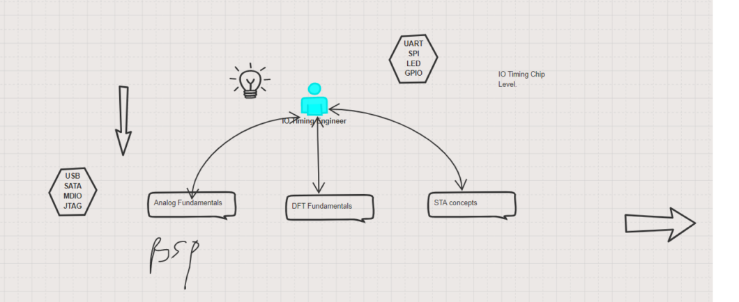
That’s it friends. I am done. My main message I want to convey is don’t worry about How many IO interfaces are there in a SOC, it can have UART, I2C, USB, LED, GPIO, blah blah blah. A few fundamentals in Analog/DFT. A bit of STA knowledge that what matters!
Thanks & Best Regards
Sriharsha Pudi @SpicaWorks