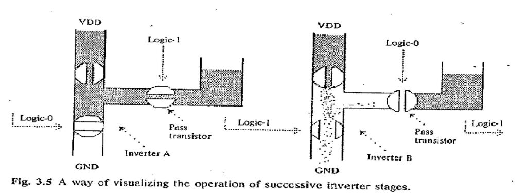
Today I want to take a different approach to answer this question. I will try to develop a Mental model to visualize the flow of current by taking an analogy with a subject like fluid dynamics, assuming the PMOS/NMOS gates as Valves that will let the water fill the tank or drain the tank from VDD to output node or from output node to GND node respectively.
Imagine logic 0 is applied to the Gates of both transistors, the NMOS valve is closed and the PMOS valve is opened, ensuring all the water gets flown from VDD to the output tank to ensure logic 1 is achieved.
Imagine logic 1 is applied to the Gates of both transistors, the NMOS valve is opened and PMOS valve is closed, ensuring all the water stored in the output tank gets drained through NMOS valve to GND node.
This is precisely how the CMOS inverter function operates.
Developing mental models and analogies is a great way of learning complex subjects.
hashtag#learningeveryday hashtag#vlsi hashtag#semiconductorindustry